

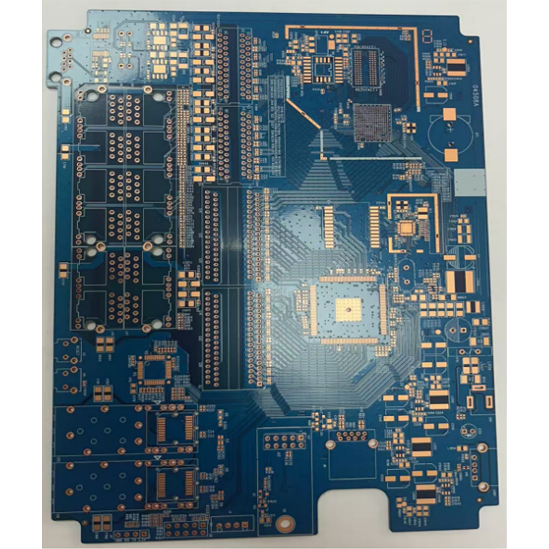
This product is a high-quality 4-layer printed circuit board (PCB)
with OSP surface finish, designed for cost-effective, high-reliability electronic applications.
The 4-layer stack-up provides stable signal routing and improved EMI performance, while the OSP coating protects copper pads from oxidation and ensures excellent short-term solderability during assembly.
Key Features
4-layer multilayer structure: Balanced performance for signal, power, and ground distribution
OSP surface finish (Organic Solderability Preservative): Thin organic coating for copper protection
Excellent solderability: Ideal for SMT and reflow soldering processes
Flat surface design: Suitable for fine-pitch and high-density components
Cost-effective solution: Lower surface treatment cost compared to ENIG or HASL
Environmentally friendly: Lead-free and RoHS compliant process
Technical Specifications
Layer count: 4 layers
Base material: FR-4 / high-Tg FR-4 (optional)
Surface finish: OSP (Organic Solderability Preservative)
OSP thickness: 0.2–0.5 μm (typical)
Copper thickness: 1 oz / 2 oz (customizable)
Board thickness: 0.6 mm – 2.4 mm
Minimum trace/space: 4/4 mil (depending on capability)
Operating temperature: -40°C to 130°C (standard FR-4)
Shelf life (before soldering): 3–6 months under proper storage conditions
Applications
Consumer electronics (smart devices, home appliances)
LED lighting systems
Industrial control boards
Communication modules
Power management circuits
Automotive electronic components (non-critical systems)
Advantages
Compared with HASL or ENIG finishes, OSP 4-layer PCBs offer:
Lower manufacturing cost for mass production
Very flat surface for fine-pitch SMT assembly
Good solderability for short production cycles
Reduced environmental impact due to organic coating
Reliable performance for medium-complexity circuits
Customization Options
Material selection (FR-4, high-Tg FR-4)
Layer stack-up design optimization
Copper thickness adjustment
Solder mask color options (green, black, blue, red, white)
Board thickness and impedance control
Panelization and assembly support
Quality Assurance
Each PCB is strictly tested to ensure production stability and performance:
Electrical test (E-test) for continuity and insulation
AOI (Automated Optical Inspection)
Impedance control testing (if required)
Solderability verification
Dimensional accuracy inspection
Microsection analysis (for quality verification)