

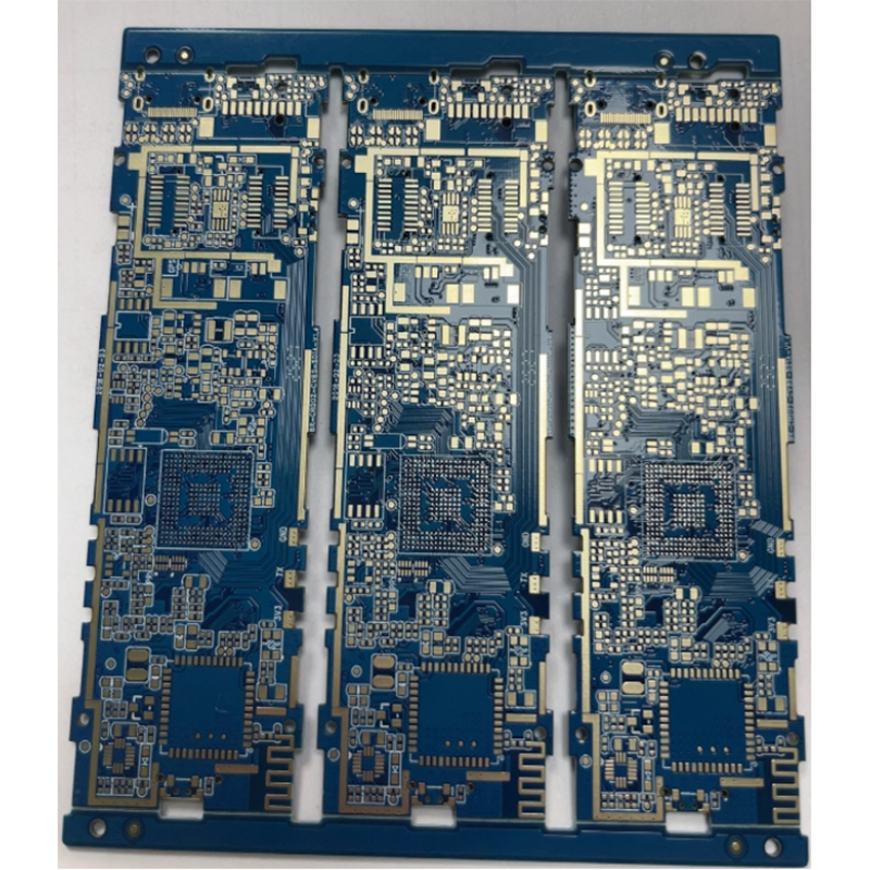
Product Overview
This product is a high-reliability 6-layer printed circuit board (PCB)
with gold-plated surface finish, designed for advanced electronic
applications requiring excellent signal integrity, durability, and
corrosion resistance. The multilayer structure enables complex circuit
routing, while the gold plating ensures superior conductivity and long-term surface stability.
Key Features
6-layer multilayer design: Supports high-density and complex circuit layouts
Gold-plated surface finish (ENIG / hard gold optional): Excellent conductivity and oxidation resistance
High signal integrity: Reduced interference for high-frequency applications
Strong durability: Suitable for long-term and harsh operating environments
Excellent solderability: Reliable SMT and through-hole assembly performance
Precision manufacturing: Tight tolerance control for advanced electronics
Technical Specifications
Layer count: 6 layers
Base material: FR-4 / high-Tg FR-4 / Rogers (optional)
Surface finish: ENIG (Electroless Nickel Immersion Gold) / hard gold optional
Gold thickness: 0.03–2.0 μm (customizable)
Copper thickness: 1 oz / 2 oz (customizable)
Minimum trace/space: 3/3 mil (depending on design capability)
Board thickness: 0.6 mm – 3.2 mm
Operating temperature: -40°C to 125°C (standard FR-4)
Applications
Communication equipment and RF modules
Industrial control systems
Medical electronic devices
Automotive electronics
Aerospace and defense systems
High-performance computing hardware
Precision instrumentation
Advantages
Compared with standard HASL or bare copper boards, this gold-plated 6-layer PCB offers:
Better oxidation resistance and longer shelf life
Improved contact reliability for edge connectors and signal paths
Enhanced performance in high-frequency and high-speed circuits
Superior surface flatness for fine-pitch components
Greater durability in demanding environments
Customization Options
Layer stack-up design optimization
Material selection (FR-4, high-Tg, Rogers, etc.)
Surface finish options (ENIG, hard gold, selective gold plating)
Board thickness and copper weight
Impedance control (single-ended/differential)
Solder mask color (green, black, blue, red, white)
Quality Assurance
Each batch is manufactured under strict quality control standards, including:
Electrical testing (E-test)
AOI (Automated Optical Inspection)
Microsection analysis
Impedance and continuity testing
Surface finish thickness inspection