

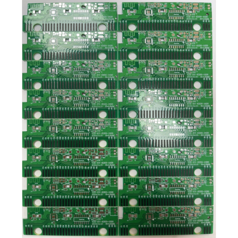
This product is a printed circuit board with carbon ink (carbon oil) surface printing, designed to provide stable conductive contact areas, wear resistance, and reliable electrical performance. The carbon ink layer is typically used on key contact regions such as keypad contacts, jumper areas, or conductive pads, offering a cost-effective and durable alternative to metal surface finishes in specific applications.
Carbon ink printed surface (carbon oil): Provides stable and durable conductive contact points
Excellent wear resistance: Suitable for repeated mechanical contact applications
Stable electrical performance: Reliable conductivity for low-current signal transmission
Cost-effective solution: Reduces the need for precious metal plating in contact areas
Good chemical stability: Resistant to oxidation and environmental aging
Compatible with multilayer PCB structures: Can be combined with FR-4 and other substrates
Board type: FR-4 PCB with carbon ink printing
Carbon ink thickness: 10–30 μm (typical, customizable)
Surface application: Selective printing on contact pads or circuits
Resistance value: Low resistance for signal/contact use (application dependent)
Base material: FR-4 / high-Tg FR-4 (optional)
Operating temperature: -40°C to 120°C (standard FR-4 range)
Adhesion strength: High adhesion to solder mask and copper surfaces
Membrane switches and keypad circuits
Remote control devices
Industrial control panels
Household appliances (control buttons)
Automotive interior electronics
Low-power signal contact systems
Flexible or rigid-flex contact designs
Compared with metal plating solutions (gold or silver), carbon ink printing offers:
Lower manufacturing cost for large-scale production
Good wear resistance for repeated pressing contacts
Stable performance in low-current applications
Reduced dependence on precious metals
Flexible design for selective contact areas
Carbon ink printing area design (full / selective / pattern-based)
Resistance control adjustment
PCB material selection (FR-4, high-Tg, flexible options)
Layer stack-up design (single-layer to multilayer integration)
Solder mask color options
Surface protection and finishing combinations
Each product is strictly tested to ensure consistent performance:
Electrical resistance testing
Adhesion strength testing
Wear resistance (rub test)
AOI (Automated Optical Inspection)
Dimensional accuracy inspection
Environmental aging testing