

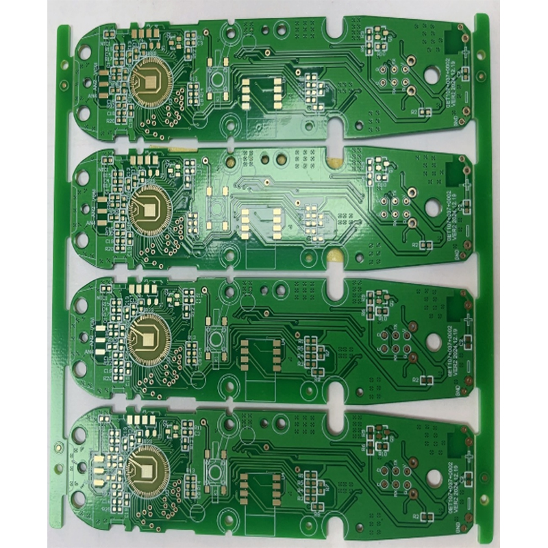
Our Double-sided Gold-Plated PCB is manufactured using advanced PCB fabrication technology and precision gold-plating processes. The gold-plated surface provides excellent conductivity, outstanding corrosion resistance, superior wear resistance, and exceptional solderability, making it ideal for high-performance and high-reliability electronic applications.
Double-sided gold-plated PCBs are widely used in communication equipment, industrial control systems, automotive electronics, medical devices, and high-end consumer electronics where stable electrical performance and long service life are required.
Typical Double-sided Gold-Plated PCB Structure:
Gold Plating Layer (Au)
Nickel Layer (Ni)
Top Copper Layer
FR-4 Substrate
Bottom Copper Layer
Nickel Layer (Ni)
Gold Plating Layer (Au)
The double-sided design maximizes circuit density while the gold-plated finish ensures superior electrical and mechanical performance.
✓ Excellent Electrical Conductivity
Gold plating provides low contact resistance and stable signal transmission.
✓ Superior Corrosion Resistance
Protects copper circuits from oxidation and environmental damage.
✓ Outstanding Wear Resistance
Suitable for repeated insertion and high-contact applications.
✓ Excellent Solderability
Ensures reliable solder joints and stable assembly performance.
✓ High Reliability
Maintains excellent performance in harsh operating environments.
✓ Long Service Life
Provides durable performance for critical electronic applications.
| Item | Specification |
|---|---|
| Layer Count | 2 Layers |
| Base Material | FR-4 |
| Board Thickness | 0.2mm – 3.2mm |
| Copper Thickness | 0.5oz – 6oz |
| Surface Finish | Gold Plating |
| Gold Thickness | Customized |
| Nickel Thickness | Customized |
| Minimum Line Width/Space | 3/3 mil |
| Minimum Hole Size | 0.15mm |
| Solder Mask Color | Green, Black, White, Blue, Red |
| Silkscreen Color | White, Black |
| Maximum Panel Size | Customized |
| Standard | IPC Class II / III |
Excellent electrical conductivity
Superior corrosion resistance
Outstanding wear resistance
Low contact resistance
Excellent solderability
Long service life
High reliability performance
Suitable for high-frequency applications
Network communication devices
RF modules
Signal transmission equipment
Base station components
Industrial controllers
Automation equipment
Precision instruments
Power management systems
Vehicle control modules
Sensor systems
Automotive communication devices
Intelligent control systems
Medical monitoring devices
Diagnostic equipment
Precision medical instruments
Healthcare electronic systems
High-end audio equipment
Smart devices
Computer peripherals
Electronic accessories